Analysis methods
The dimensional accuracy analysis
In addition to its electrical properties, each PCB has the function of a mechanical component carrier and is usually also used to secure the complete assembly in an enclosure after it has been assembled. Therefore, the dimensions and drill diameters are of elementary importance for the usability.
In times of innovative CNC technology, we use high-precision automatic drilling, milling and laser machines for mechanical processing that deliver reproducible results hundreds of thousands of times over. Nevertheless, it is essential to check these results. For this purpose, ILFA uses state-of-the-art coordinate measuring technology.


We measure the contour of your PCB optically with a 2-coordinate measuring machine, and we check the drill diameters using the transmitted light method. We can also approach and measure breakouts in the PCB, special PCB geometries or individual drill positions with pinpoint accuracy if the dimensions are critical. We document and evaluate the results of the dimensional accuracy analysis for you in the test report in tabular form.
The cut analysis
One of the tests we carry out most frequently in our laboratory is the microsection analysis to assess structural integrity. This is a destructive test in which we assess the quality of vias, blind vias (blind holes) or burried vias (buried holes), among other things.
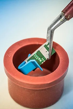
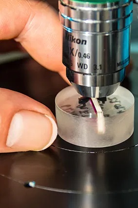
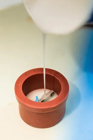
To do this, we take a coupon from a PCB of your order and embed it in a transparent two-component resin. We then prepare the sample with wet sandpaper of various grit sizes on a rotating sanding disc. The grinding ends in a polish with a diamond emulsion with a grain size of 1µm. We can work out the crystalline structure of the different copper layers with an additional preparation step to make the structure of the metallisation visible.
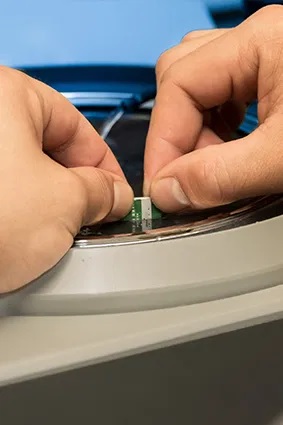
We evaluate the ground sample under a light microscope with a digital camera system. The quantitative characteristics of a multilayer PCB documented in your analysis report are usually:
- Copper layer thickness of the metallisation of the smallest unfilled hole (drill sleeve).
- Copper layer thicknesses of the outer and inner layers.
- Insulation layer thicknesses (prepreg and core layers).
- Lacquer layer thickness on the trace edge and on the base material.
- Total layer thickness of the final surface (e.g. ENIG).
If you wish, we can also display the conductor track widths of structured inner layers in the micrograph, which can be useful for checking the specifications for controlled impedances, for example. sein kann.
The impedance measurement
For proper signal transmission in high-speed PCBs, the measurement of the controlled impedance is just as important as the electrical connection test. If the impedance actually achieved deviates significantly from the previously calculated impedance, this has a decisive influence on the signal integrity of the assembly. The consequences are reflections in the transmission line and switching signals that are applied to the components at the wrong time.
For the impedance measurement we use the TDR method (Time Domain Reflectometer). We carry out the measurement on a coupon that is placed in the production slot of the PCB and replicates the circuit path structures of the PCB.
With the TDR we send a pulse with a short rise time into the coupon and measure the reflections of the pulse in the defined transmission line. From the reflection behaviour, direct conclusions can be drawn as to whether the calculated target impedance is reached. The result of the impedance measurement is included in your delivery documentation in the form of a measurement report for each individual coupon.
The electrical test
The essential purpose of the PCB is the electrical connection of defined component connections of a common potential and the reliable isolation of different electrical potentials. Which component connections must be interconnected is described in the netlist of the assembly. If we have not received a netlist with your production data, we generate our own netlist from our CAM data and test the electrical function against it.
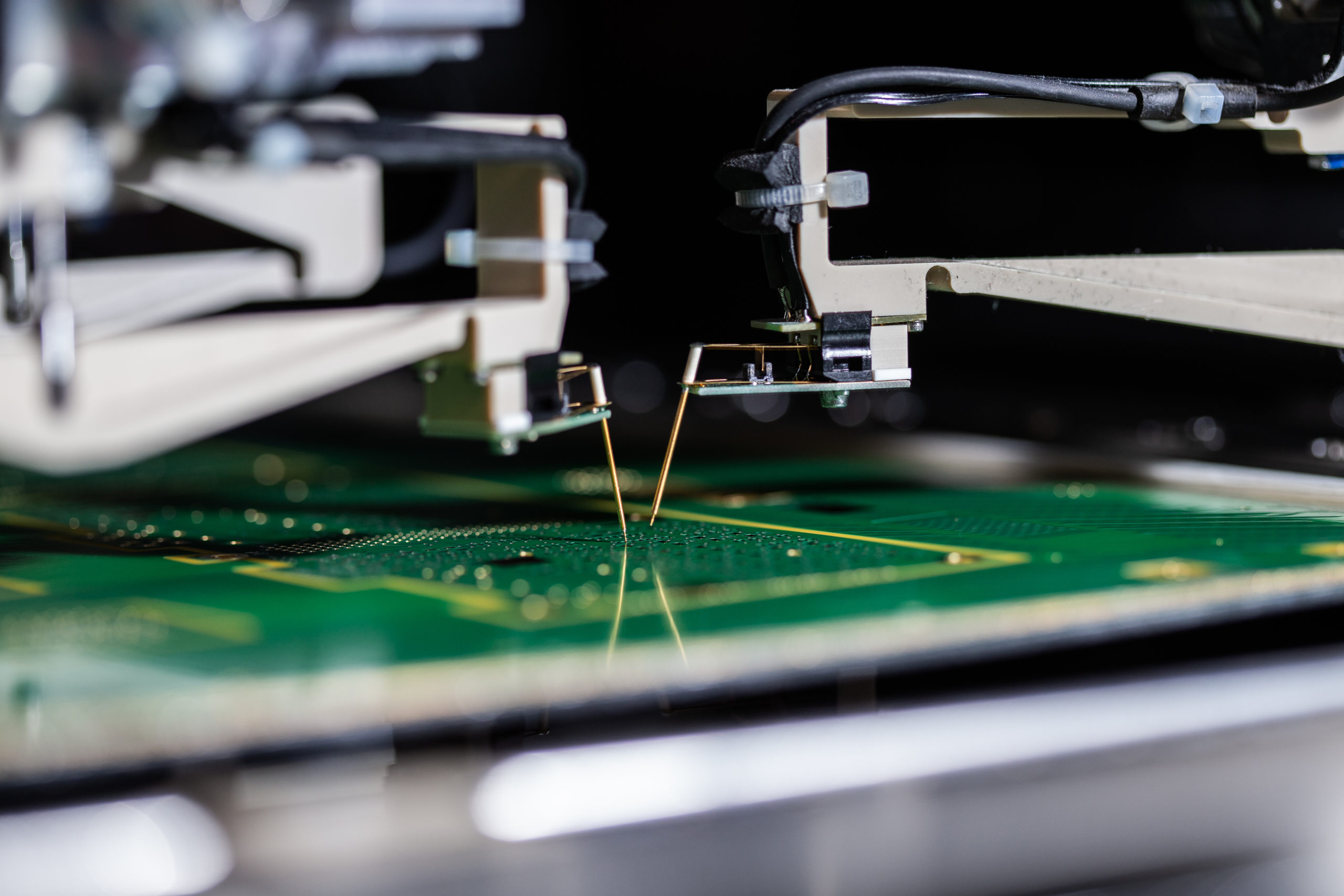
For the bare board test, we at ILFA use so-called finger testers (Flying Probe Test). These devices have moving, numerically controlled probes with which defined test points on the top and bottom of the PCB are approached and contacted. The test programme in this case is the virtual test adapter, which makes it possible to carry out both short-circuit tests and connection tests with previously set parameters.
In the test report, we document the test conditions (test voltage and resistance threshold values) and the passing of the E-test for you. This way you can see at any time which employee tested the PCBs on which test equipment and how many of the tested PCBs passed the test.