Technology
We are familiar with the most modern technologies in order to be able to offer our customers optimal support in the production of printed circuit boards. Our spectrum includes all services from CAD design to the creation of PCB prototypes and production tools to long-term documentation and data backup. We are continuously working on improving our production methods and the materials used. What counts for us is that we are already prepared today for our customers’ future product ideas.
Industries
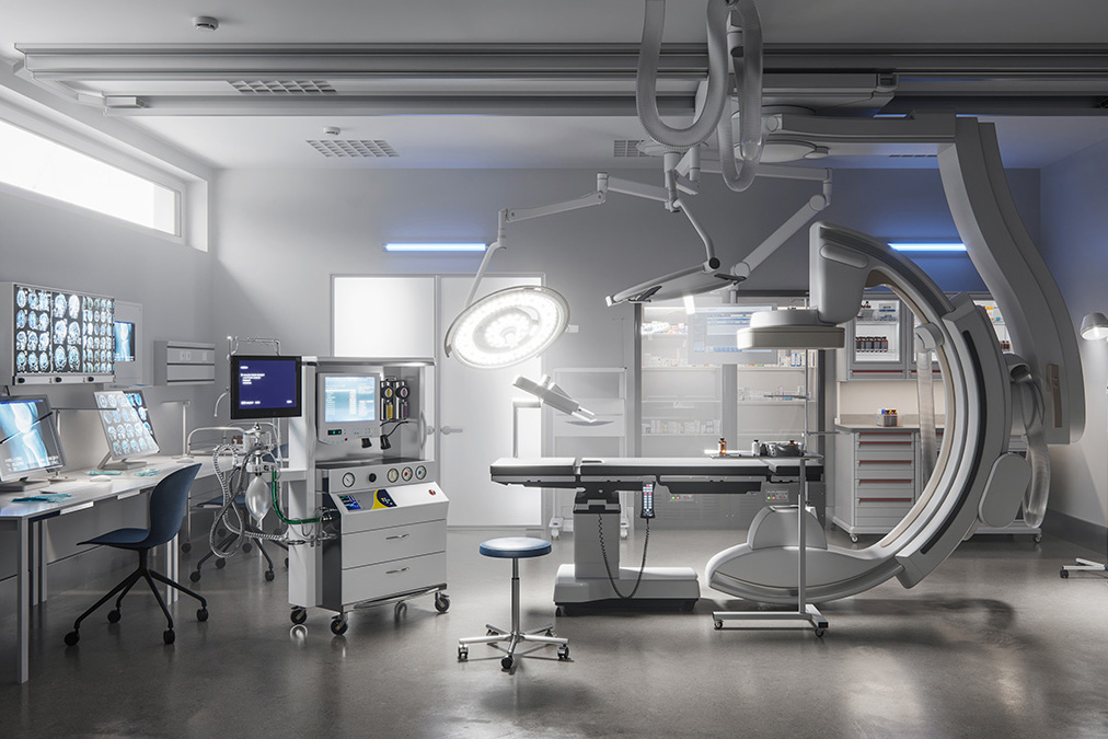
Our customers are at home in a wide range of industries. We produce printed circuit boards for special applications in the electronics industry, medical technology, aerospace and defence technology. From global players to research institutions and start-ups, we fulfil all the requirements that our customers place on modern printed circuit boards.

Our technological range:
- Rigid, Flexible and Rigid-Flex PCBs
- Ultra Thin Multilayers
- Blind, buried, stacked vias / Plugging
- HDI-PCBs
- Impedance controlled traces
- Microfine PCBs up to 50 µm
- Embedded Components
- Integrated micro cooling system (ILFACOOL)
- HF and power technology
- EMC-compliant PCBs
- Material hybrid structures
- Edge metallisation
- Single and double-sided PCBs
- Electro-optical printed circuit boards
- Multilayer up to 32 layers
Our services at a glance:
- Prototypes or small and medium series
- Large series via certified ILFA partners or coordination of prototype production with processes of the customer’s service provider
- CAD design
- Scan service for non-digital film material and creation of Gerber data
- Layout review and feasibility analysis
- Assembly via partner companies
- Takeover of documentation and backup of data for at least 10 years
- Preparation of test reports
- Analyses and test procedures in our own laboratory
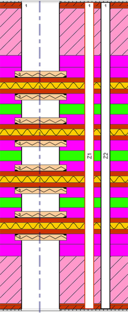
Hybrid superstructures are our speciality
Modern assemblies often have to combine different properties. This often lends itself to a hybrid layer structure. Let us talk about your requirements! Thanks to our experience, we can always offer you the best possible solution.
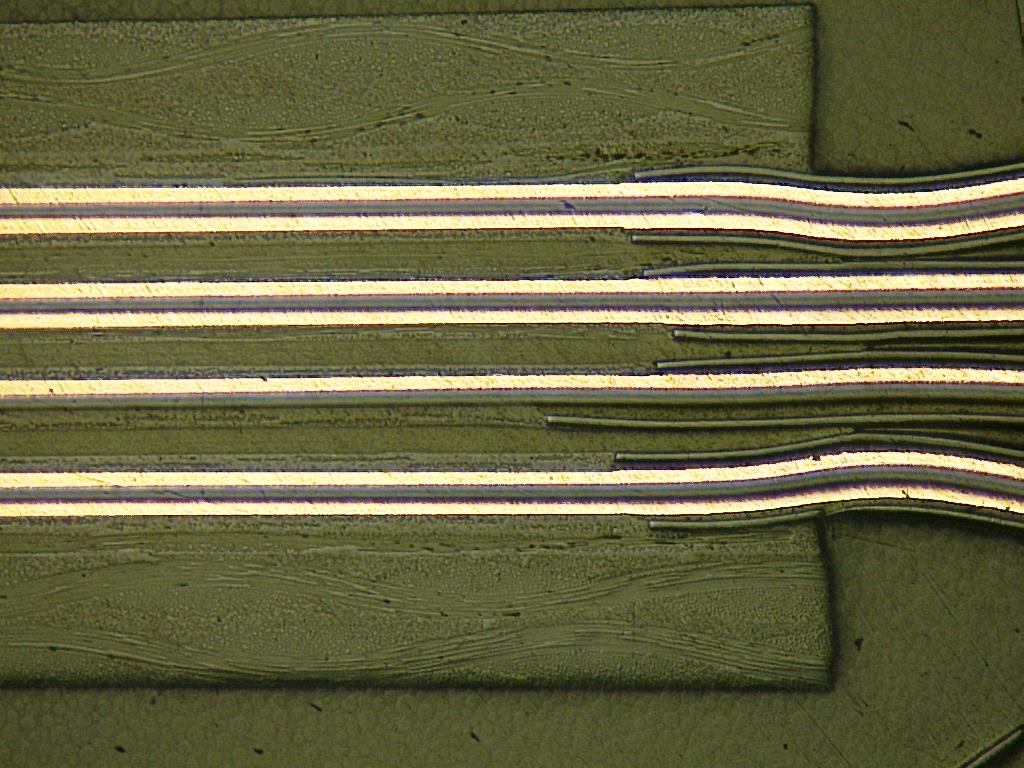
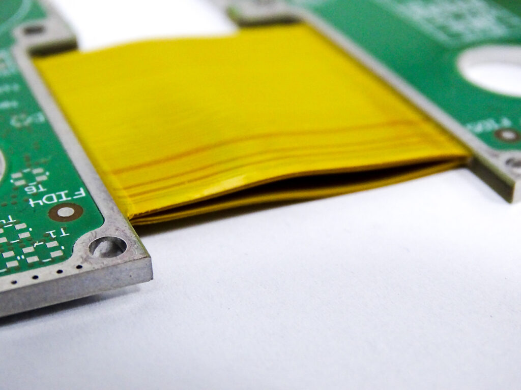
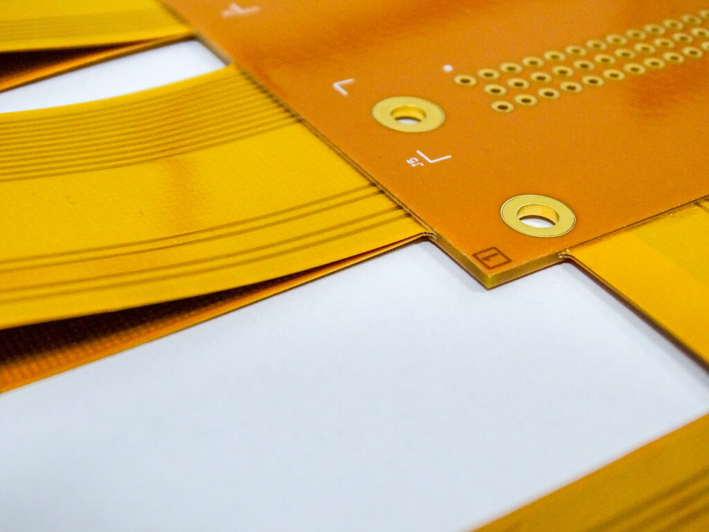
Rigid-flex core competence
Rigid-flex PCBs are right up our street! Rigid-flex PCBs, also known as flexible PCBs with rigid sections, offer an advanced solution by combining conventional “rigid” PCBs with flexible sections. This unique design makes it possible to replace several separate rigid PCBs that would otherwise have to be interconnected by cables. Often, the rigid-flex PCB is a cost-effective alternative.
Avantages of Rigid-flex PCBs
- Reduced installation time: The use of rigid-flex PCBs can often significantly reduce installation time as fewer connections and cabling are required.
- Saving on components: By integrating flexible areas into the PCB, various components such as connectors, cables and additional PCBs can be saved, resulting in a more efficient assembly.
- Greater miniaturisation: Rigid-flex PCBs enable better utilisation of the available space and promote the miniaturisation of electronic devices.
- Improved reliability: As there are fewer connectors, the reliability of the assembly increases. Plug contacts are often prone to contact problems, especially when the flexible area is subjected to dynamic bending stress, which is less relevant with rigid-flex PCBs.
- Although the production of rigid-flex PCBs can be somewhat more expensive due to their complex structure and the use of different materials, in many cases the advantages outweigh the disadvantages when all actual, effective and imputed costs are taken into account.
In terms of materials, rigid-flex printed circuit boards consist of a hybrid structure. The rigid areas are made of conventional FR4 material, while the flexible parts are made of polyimide. These materials have different bendability and thermal expansion properties, which must be taken into account during production. One challenge is to take into account the different thermal expansion behaviour of the materials before pressing to ensure that the multilayer composite fits precisely.
The manufacturing process begins with the production of the FR4 cores, which are manufactured in a similar way to multilayer boards. At the same time, one or more flex cores are produced from polyimide. All layers are then brought together in a pressing process to form a rigid-flexible composite, using special low-flow or no-flow prepregs as the composite material.
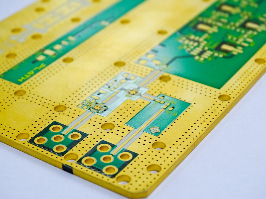
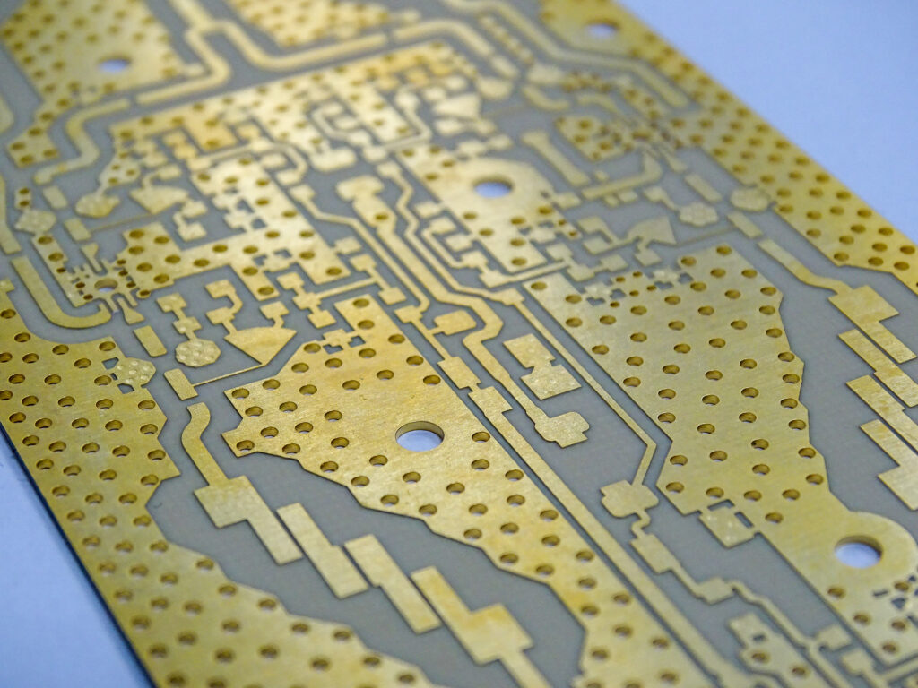
HDI printed circuit boards
High circuit densities in combination with short signal paths and low space requirements can be realised in PCB production with HDI PCBs. HDI stands for “High Density Interconnect” and fulfils the requirements for ever greater performance and compact design in digital end devices.
In order to achieve the high circuit densities, laser systems are increasingly being used instead of mechanical drilling tools for through-hole plating of the PCBs. This allows drilling diameters of 50 µm to be realised in large quantities, even as blind vias, in a short space of time. It is particularly important to achieve the greatest possible precision between the drilling pattern and the conductor pattern in order to minimise offset problems with residual rings of 50 µm.
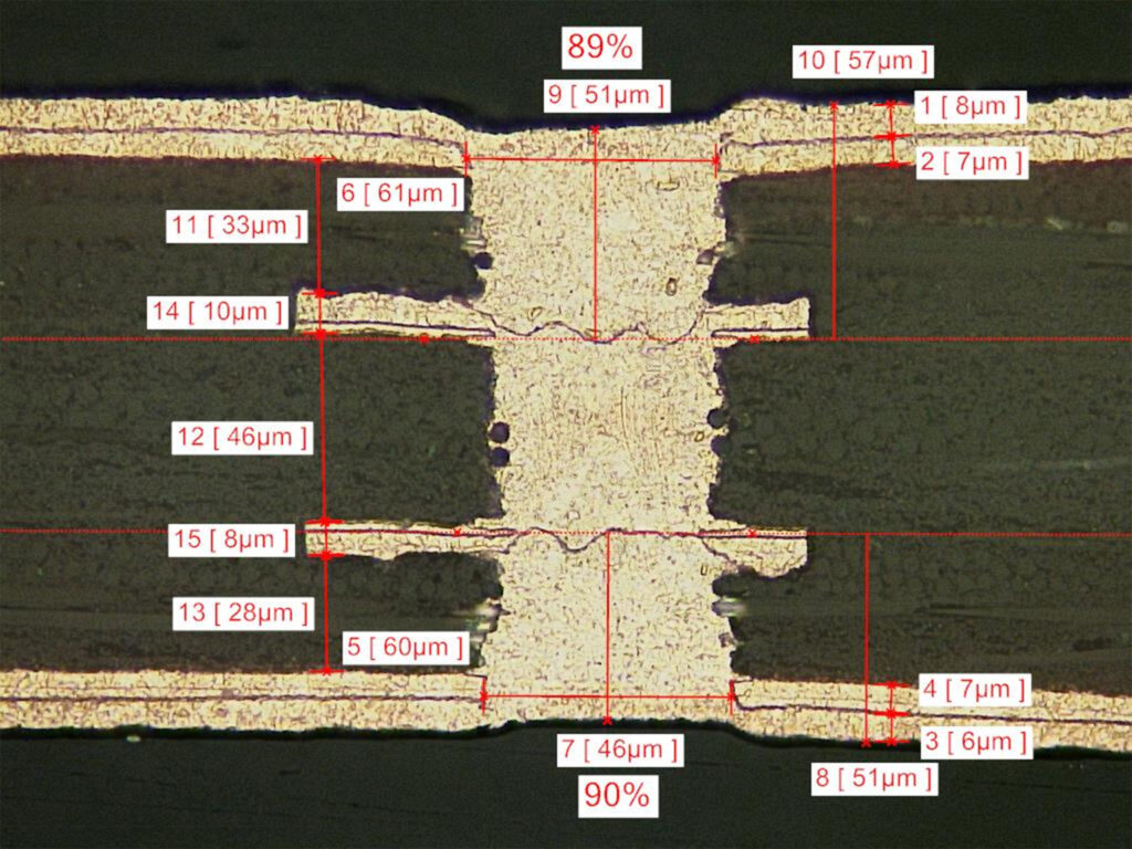
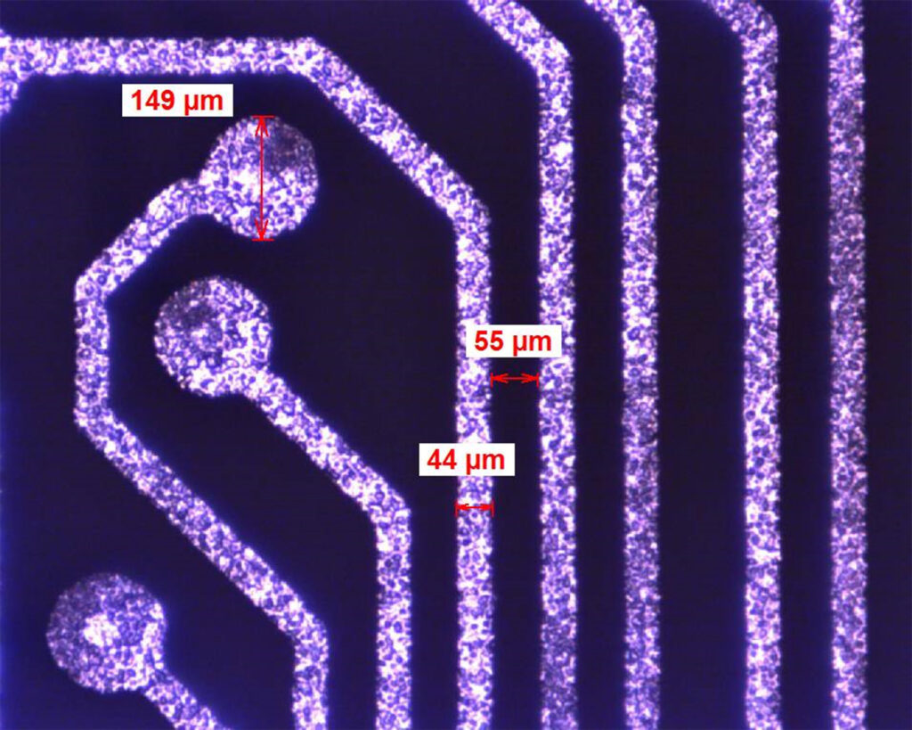
This is ensured at ILFA with a sequential manufacturing process optimised for fine structures, with which drilling and exposure offsets in Anylayer construction types can be reduced on average to +/-10 µm.
HF-Hybrid
Whenever a high degree of signal integrity is required, but at the same time less demanding circuit parts must be combined within one assembly, a hybrid construction is recommended. A combination of materials, e.g. FR4, ceramics and Teflon, can be worthwhile, because it is not uncommon for the cost of high-frequency substrates to be more expensive by a double-digit factor than basic material FR4.
Special properties of the PCB
With a hybrid construction, special properties can be given to the PCB areas that come into contact with the environment. Common requirements include low outgassing properties, low moisture absorption, special expansion properties or increased thermal conductivity.
XY-Hybrid
Conventional hybrid PCBs are limited to the layer-by-layer (Z-direction) use of different materials. In order to offer our customers more individual development options, we have developed a process that allows us to change the base materials within a PCB in the X/Y direction as well.
Research and development
We constantly have exciting and innovative research projects, such as e2LEAD. In this project, we are developing an electronics system with particularly high reliability for autonomous driving.