Technologies and processes at ILFA: Sophisticated HDI design in PCB production
The requirement for high circuit densities in combination with short signal paths and low space requirements can be realised in PCB production with so-called HDI PCBs. HDI stands for “High Density Interconnect” and, as a relatively new technology, plays an important role for ILFA GmbH in fulfilling demanding customer requirements. The increasing miniaturisation of digital end devices goes hand in hand with the simultaneous pursuit of ever higher performance and ever more compact design, which can be seen as a technically demanding challenge for the manufacturers of the corresponding printed circuit boards. A challenge that we are naturally happy to accept!
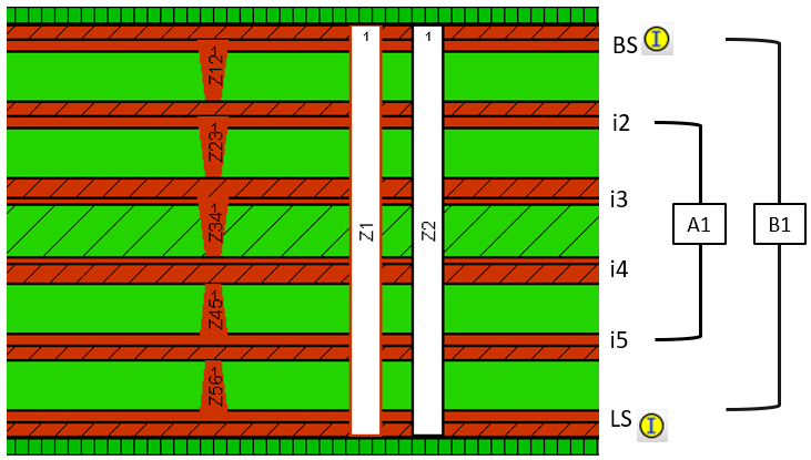
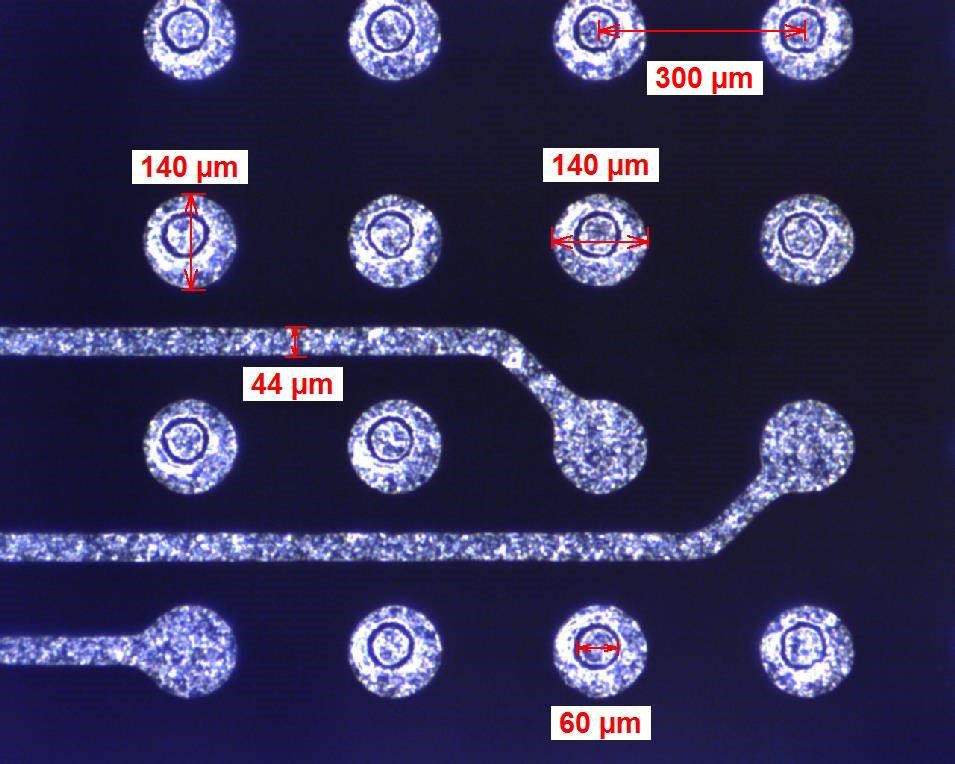
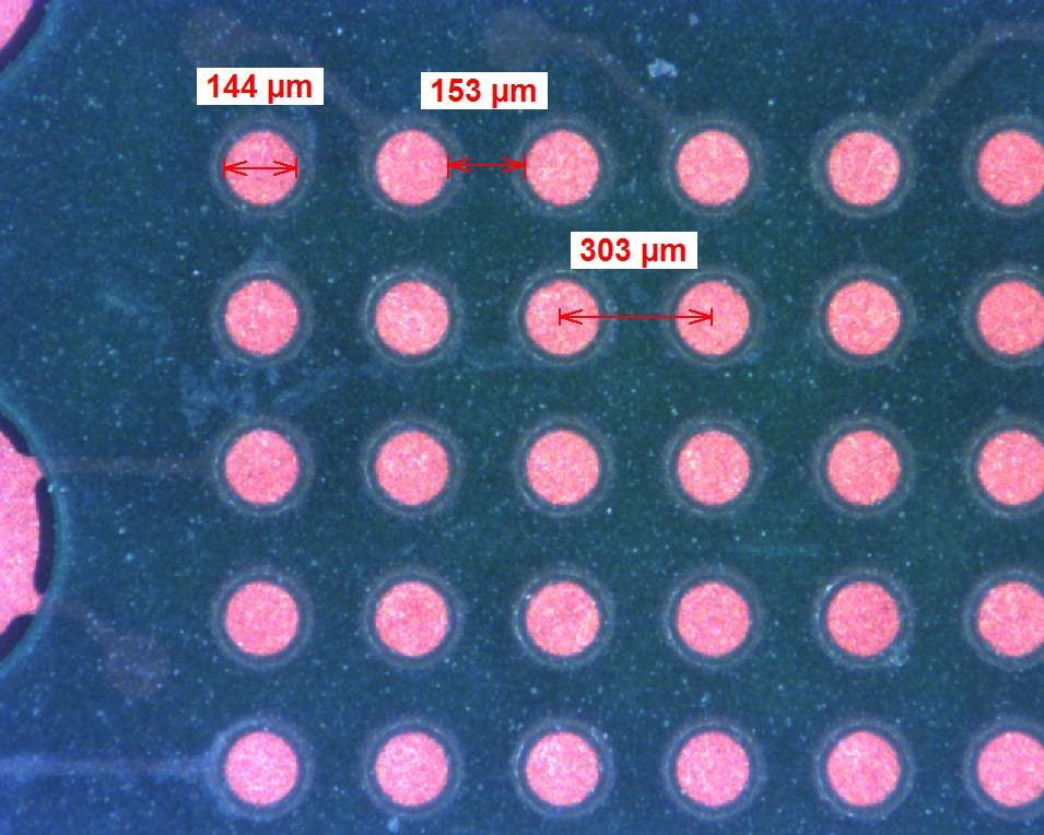
One such case for ILFA was a customer request for a sequential assembly with 6 electrical layers, as shown in Figure 1. The customer requirement included 50 µm line/space on all layers, in combination with 300 µm BGA pitch on the outer layers, as well as a smallest pad diameter of 150 µm.
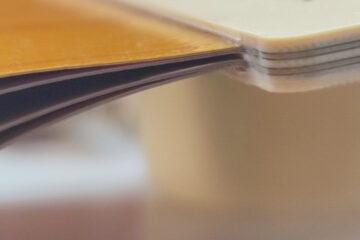
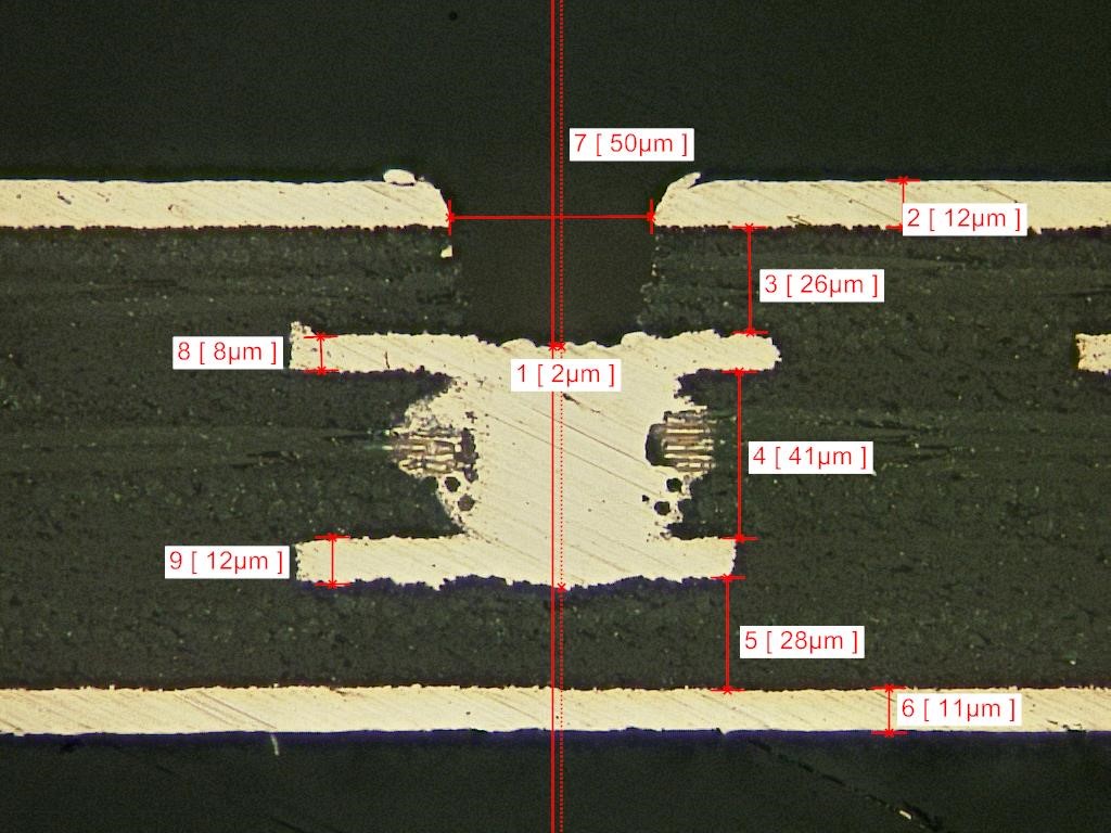
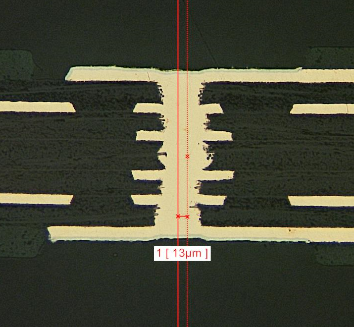
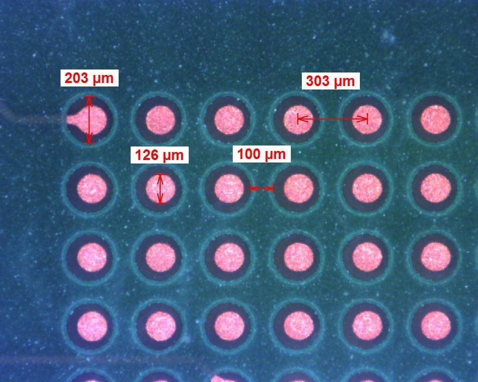
The through-hole plating was realised using 50 µm laser vias in order to hit the target pad of the underlying layer with the highest possible probability. The maximum permitted offset of 50 µm between the drill pattern and the conductor pattern meant that new approaches were required for the registration systems during drilling and exposure. The single card alignment provided the most accurate results with an offset between the hole pattern and the conductor pattern on the same layer of up to a maximum of 30 µm over the entire surface of the production format. The 50 µm laser vias were realised using a UV laser. The result of the stacked laser vias can be seen in Figure 2. The offsets were reduced to a minimum thanks to the individual card processing.
A homogeneous copper layer thickness distribution on the surface is essential for a uniform etching result of the fine structures in the conductor pattern. This was achieved by a special galvanic deposition process, whereby a total thickness of the copper layer of 20 µm is not exceeded even after the copperfill, and is deposited with a measured accuracy of +/1 µm. The via between layers 3 and 4 was electrolytically filled using the THF (Through Hole Filling) process. The conductor pattern is then structured (Figure 3).
Once the conductive pattern has been finalised, the solder resist mask is applied using a spraying process. The 150 µm resist clearance in the BGA area is a particular challenge here. Particular attention must be paid to the positioning accuracy in relation to the conductor pattern and the contour sharpness after exposure and development. In this case, too, local alignment of each individual board was used to maximise exposure accuracy.
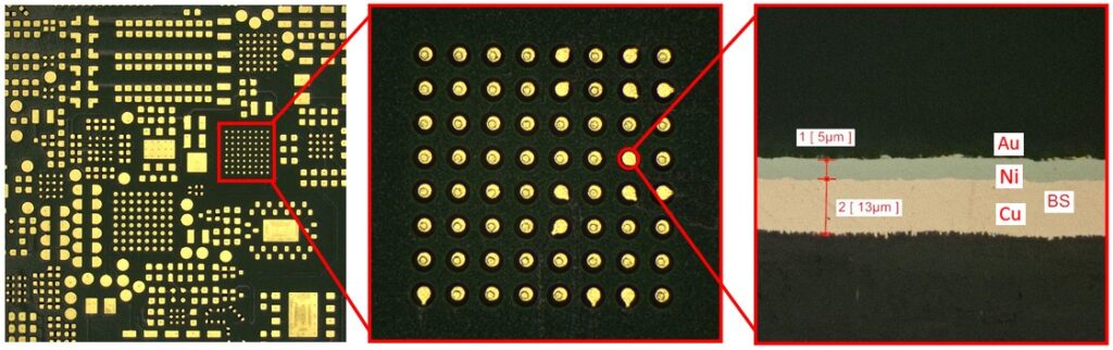
To protect the copper surface from oxidation and to increase the wettability of the connection surfaces during soldering, a final surface is applied to the PCB, in this case ENIG (electroless nickel immersion gold) as shown in Figure 5. This layer consists of 4.0 – 6.0 µm nickel and a 0.06-0.12 µm thick layer of gold. Due to the chemical deposition process and the absolutely flat surface, it is ideally suited for the fine-pitch application on this PCB.
In the meantime, we have already successfully realised this order several times, so that the processes are firmly defined. Do you also have a challenging project? Feel free to contact us, we look forward to your enquiry!
Responsible for content: Nikolas Koulouris