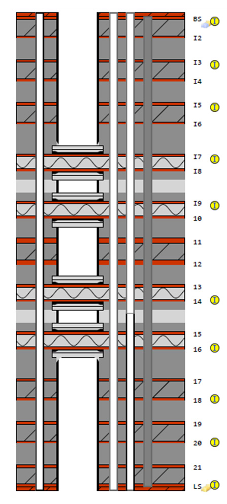
Technologies and processes at ILFA: High-frequency printed circuit board with four flex layers
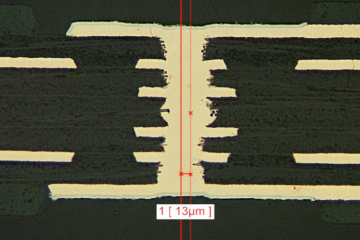
One of our current projects is intended for use as a high-frequency application. The requirements are correspondingly high, which, in addition to high-frequency suitability, envisage a rigid-flex PCB design with four flexible layers. The via fill and backdrilling processes are also used. Backdrilling or reverse drilling is a proven method for removing vias from a specific layer of a multilayer PCB. Unnecessary layer vias are removed in order to eliminate unwanted reflections, which can lead to signal distortion and lower performance. The diameter of the backdrill is usually larger than the diameter of the via.
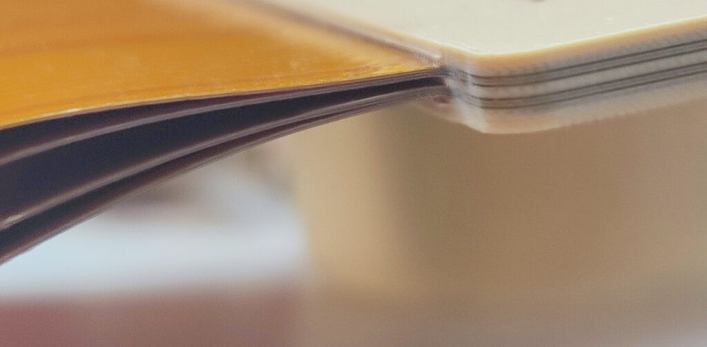
A high-frequency-compatible material was used for the realisation (dielectric constant @10 GHz =3.38, dissipation factor @10 GHz =0.0028). Polyimides and a NoFlow prepreg were used for the hybrid structure.
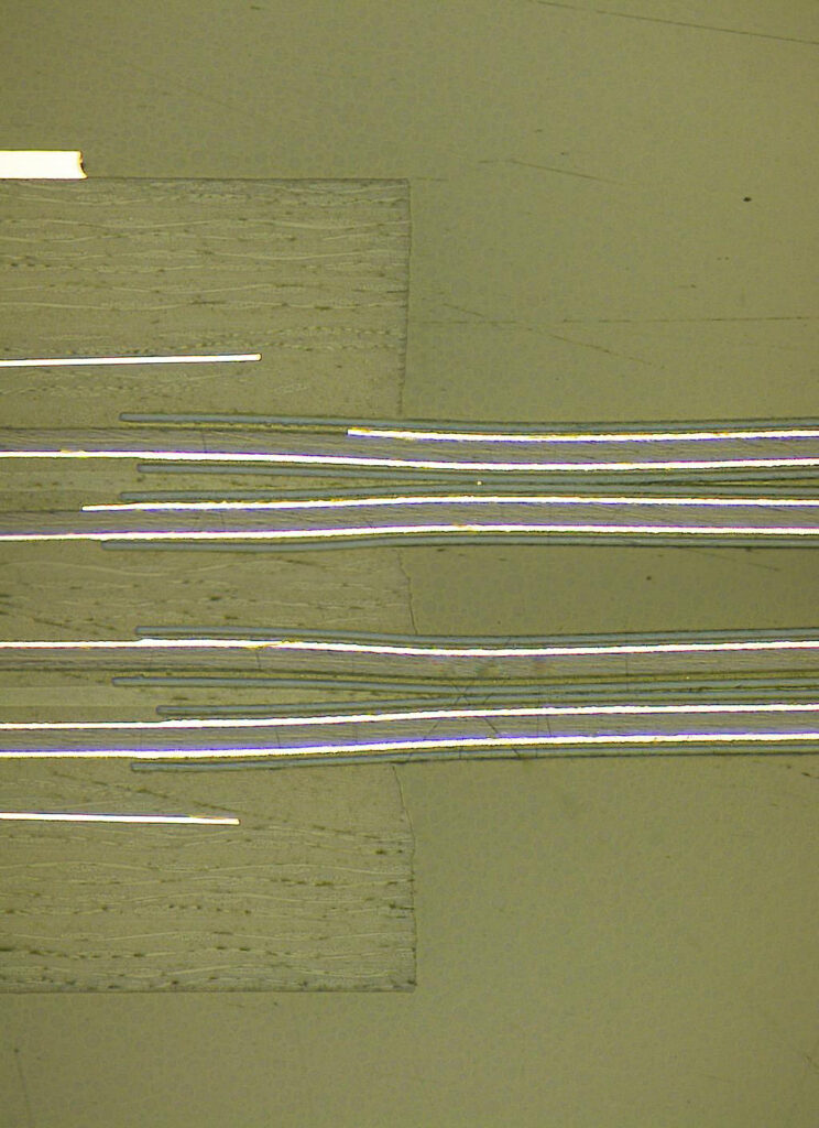
The end result for our customer is a PCB with optimised rigid to flex transitions (Fig. 3) and high-frequency suitability is guaranteed.
Do you also have special requirements and specifications for your project that need to be met? Please contact us and we will work out an individual solution that is optimised for your area of application.